半导体切片
Precision Diamond Wire Cutting for Solar Wafer Production
High-efficiency N-type and P-type solar wafers are the core of next-generation photovoltaic modules. Precision diamond wire cutting is critical to producing ultra-thin, high-quality wafers that maximize cell conversion efficiency and material yield. This process has replaced traditional sawing, delivering lower kerf loss, higher throughput, and superior surface quality for mass PV manufacturing.
Our diamond wire systems ensure consistent wafer thickness, minimal breakage, and controlled surface damage, enabling high-throughput production of ultra-thin wafers while meeting the strict quality requirements of modern solar cell technologies.
Precision Diamond Wire Cutting for High-Efficiency Solar Wafers
Our diamond wire cutting solutions are tailored for high-efficiency PV wafer production, delivering ultra-thin, high-quality wafers that directly boost solar cell conversion efficiency. The systems feature advanced wire path optimization and real-time monitoring, ensuring consistent thickness, flatness, and surface quality for N-type TOPCon, HJT, and other next-generation solar cells. With low-damage cutting technology, they minimize wafer warpage and micro-cracks, significantly improving cell yield and module performance.
高效光伏晶片加工
Core Benefits
- Ultra-Thin Wafer Capability: Achieve stable slicing of wafers as thin as 100μm, reducing silicon usage and lowering cell costs.
- Superior Surface Quality: Low-damage cutting eliminates the need for extensive post-processing, simplifying production steps.
- High Yield & Low Breakage: Intelligent cutting algorithms reduce wafer breakage rate to below 1%, maximizing production yield.
- Energy & Cost Savings: High-efficiency cutting design reduces power consumption per wafer, cutting operational expenses.
Application Scenarios
- High-efficiency N-type/P-type solar wafer manufacturing
- Ultra-thin wafer processing for HJT, TOPCon, and IBC cells
- Wafer slicing for bifacial and high-power PV modules
技术规格
| 不. | 参数 | 规格 |
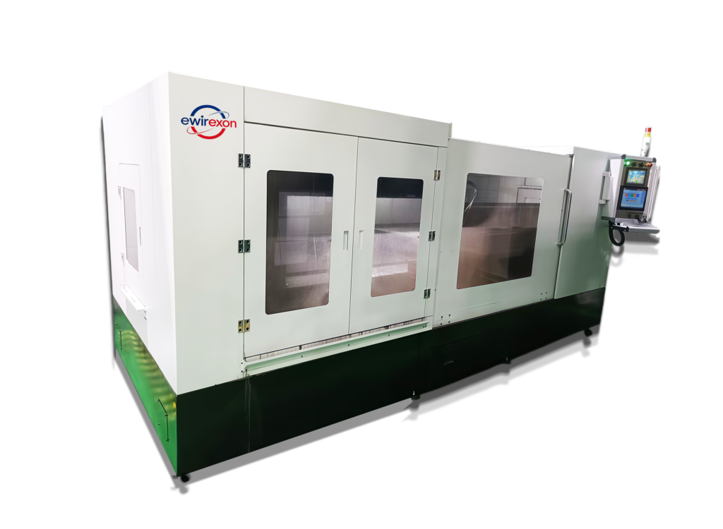
| 1 | 模型 | TCQF15030CNC |
| 2 | 切割原理 | 无尽金刚石线/物理切割 |
| 3 | 切割功能 | 切片/二维轮廓切割 |
| 4 | 最大工件尺寸(毫米) | 1200 × 1000 × 1000 毫米(长×宽×高) |
| 5 | 工作台尺寸(毫米) | 1500×300 |
| 6 | 切割平面精度(毫米) | 0.1 |
| 7 | 表面粗糙度(μm) | Ra 0.8 μm |
| 8 | 电线规格(毫米) | Ø0.65-1.0/6250 |
| 9 | 张力系统 | 恒线张力控制 |
| 10 | 导轮数量 | 4 轮 |
| 11 | 驱动电机 | 伺服电机 |
| 12 | 线速(米/秒) | 51Max(可调) |
| 13 | 总功率 | 3.6 |
| 14 | 电压 | 220 伏 50 赫兹 |
| 15 | 控制系统 | 定制开发的通程 T33 系统 |
| 16 | 占地面积(长×宽×高)(毫米) | 3200×1500×1500 |
| 17 | 毛重 千克 | 3200 |